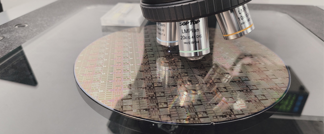
As a manufacturer deeply rooted in the optical inspection field, Handing Optics has an in – depth understanding of the “fastidiousness” in the semiconductor industry. In this world measured by microns and nanometers, the slightest error can potentially affect product performance. Today, let’s explore how our metallographic tool microscopes help customers solve those “invisible challenges”.
1. “Health Check” for Wafer Fabs
Wafer manufacturing is like cultivating crops, where every process requires meticulous attention. Take the photolithography process for example. If the line width deviates by one – thousandth of a hair’s breadth, the chip may be scrapped. Our microscope, acting like an “electronic eye”, can magnify the wafer surface up to 2000 times, clearly revealing even the tiniest pits as small as 0.1 microns. After a customer used our equipment, they were able to directly detect the hidden micro – cracks in the grinding process, and the yield rate increased by a whopping 40%!
2. “Magnifying Glass” for Packaging and Testing
Chip packaging is like putting on protective clothing for delicate chips. Our microscope can not only clearly observe whether the solder balls are of uniform size but also “see through” to check for internal voids. A customer engaged in advanced packaging used to rely on manual sampling inspection, which was inefficient and prone to missed detections. Now, with our automatic measurement software, they can measure 1000 solder balls in just 3 minutes, and the defective product detection rate has soared to 99.9%!
3. “Problem – Solving Magic Tool” for Failure Analysis
What should you do when a chip malfunctions? Our microscope is like a detective, capable of finding clues in the microscopic world. Once, a customer’s chip had an inexplicable short – circuit. Through our microscope, we discovered that an internal gold wire was broken. After conducting a component analysis, we found that the material impurity exceeded the standard. The customer adjusted the process according to our report, and similar problems never occurred in subsequent products.
Why Choose Us?
Sharp Vision: We use the same apochromatic objective lenses as research institutions, ensuring clear views of everything.
Quick – witted Brain: Our AI algorithm can automatically identify abnormal points, which is 8 times faster than manual detection.
Robust Build: We’ve specifically designed an anti – vibration base, enabling the microscope to remain stable even in a workshop environment.
Our Sincere Words
Friends in the semiconductor industry often say, “A miss is as good as a mile.” What we do is transform this “tiny difference” into “clairvoyance” – from R & D to mass production, helping you keep every detail in sight and under control. If you’re also troubled by microscopic inspectio, feel free to come and talk to us. Maybe we’ll strike up a unique spark!
Handing Optics – Making the Tiny Visible and Precision Controllable!
Post time: Mar-07-2025